Pictures added
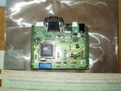
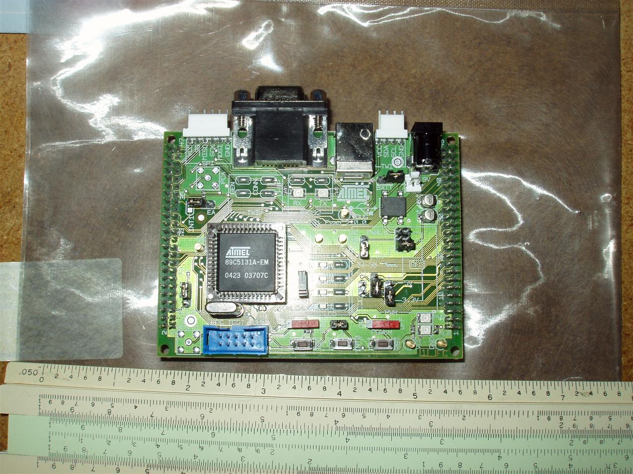
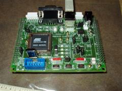
OK, here are some pictures of the latest schematic and PCB layout top, bottom, and top+silkscreen layers. The size of this board is 2"x2", as stated in the previous post. There might be some minor tweaks to this, but it shouldn't be too drastic.
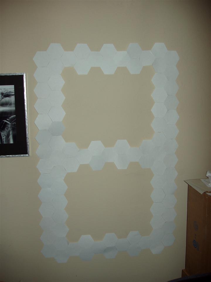
Here's a pic of what the hexagon wall currently looks (1:1 scale made with paper). The center would obviously be filled, and this is 11x14.5 pixels:

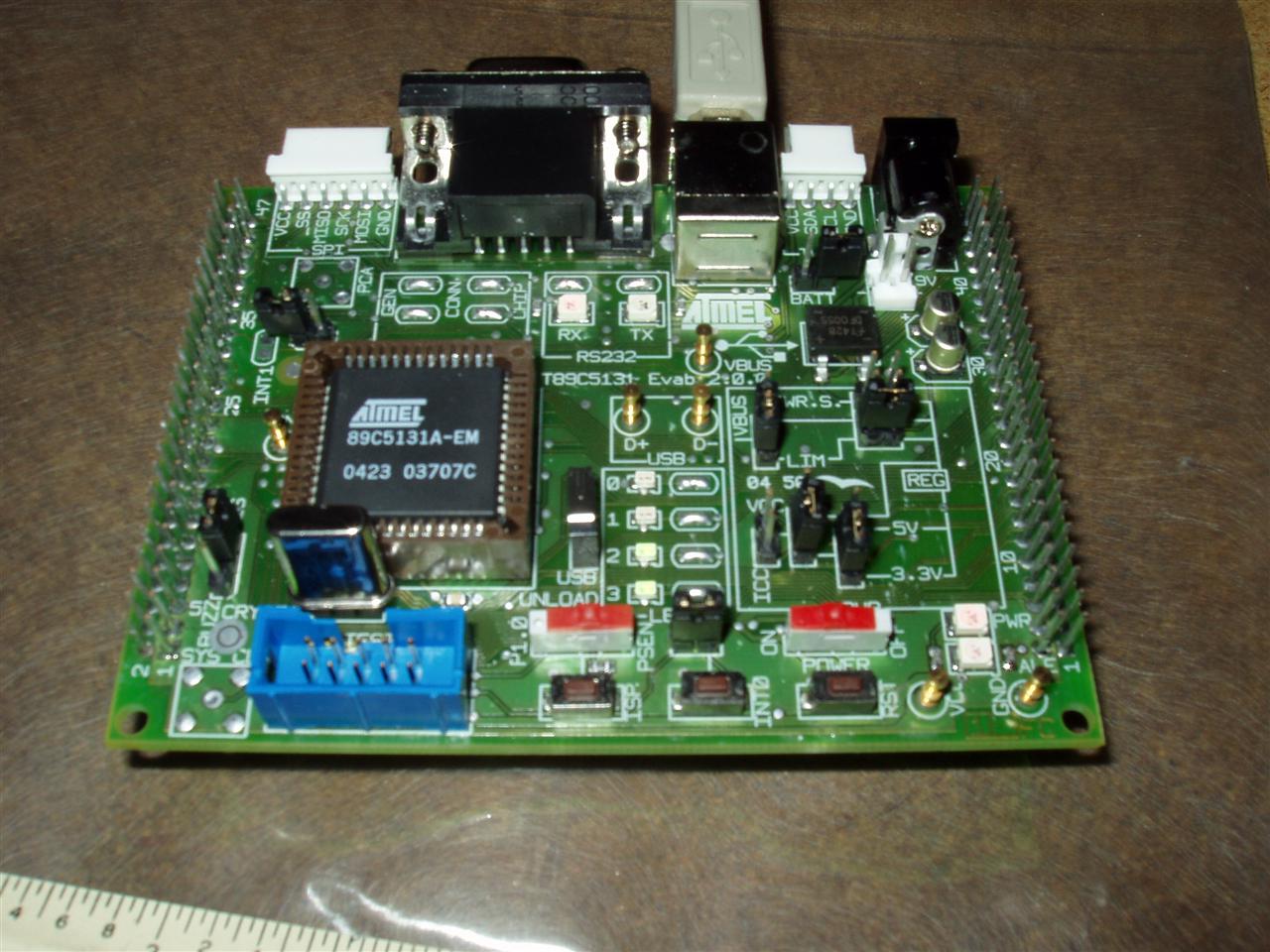
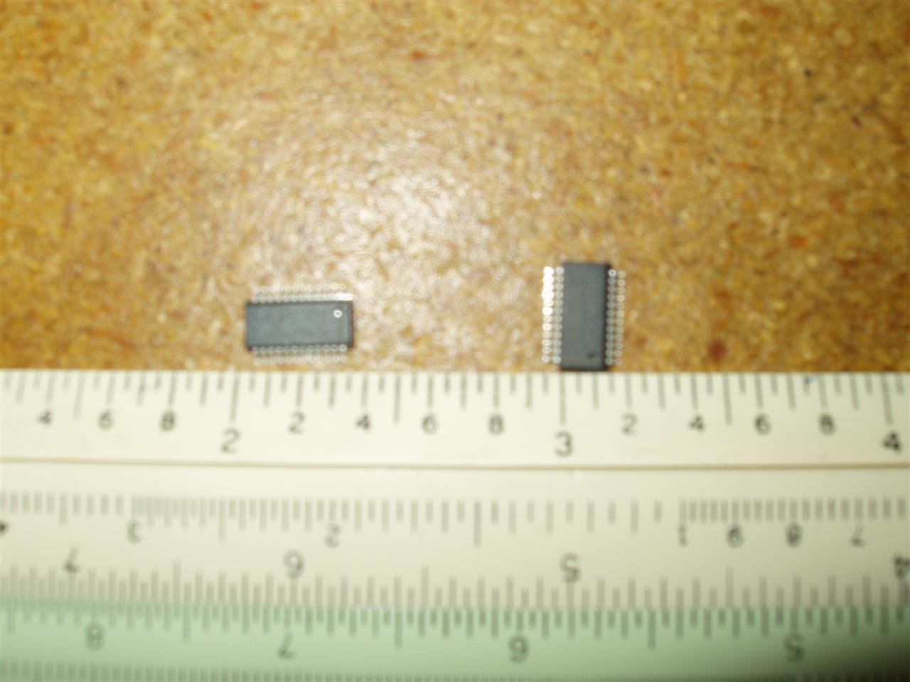
Here's a couple more pics, of the board and the engineering samples of the LED driver chips I received. Yes, 32 of those tiny chips need to be soldered! Markings on the ruler are inches, with tenths of inches in-between.
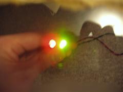
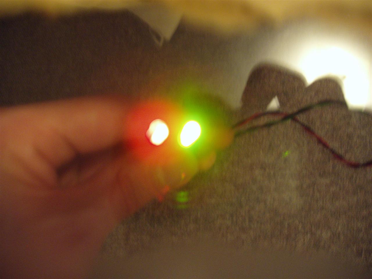
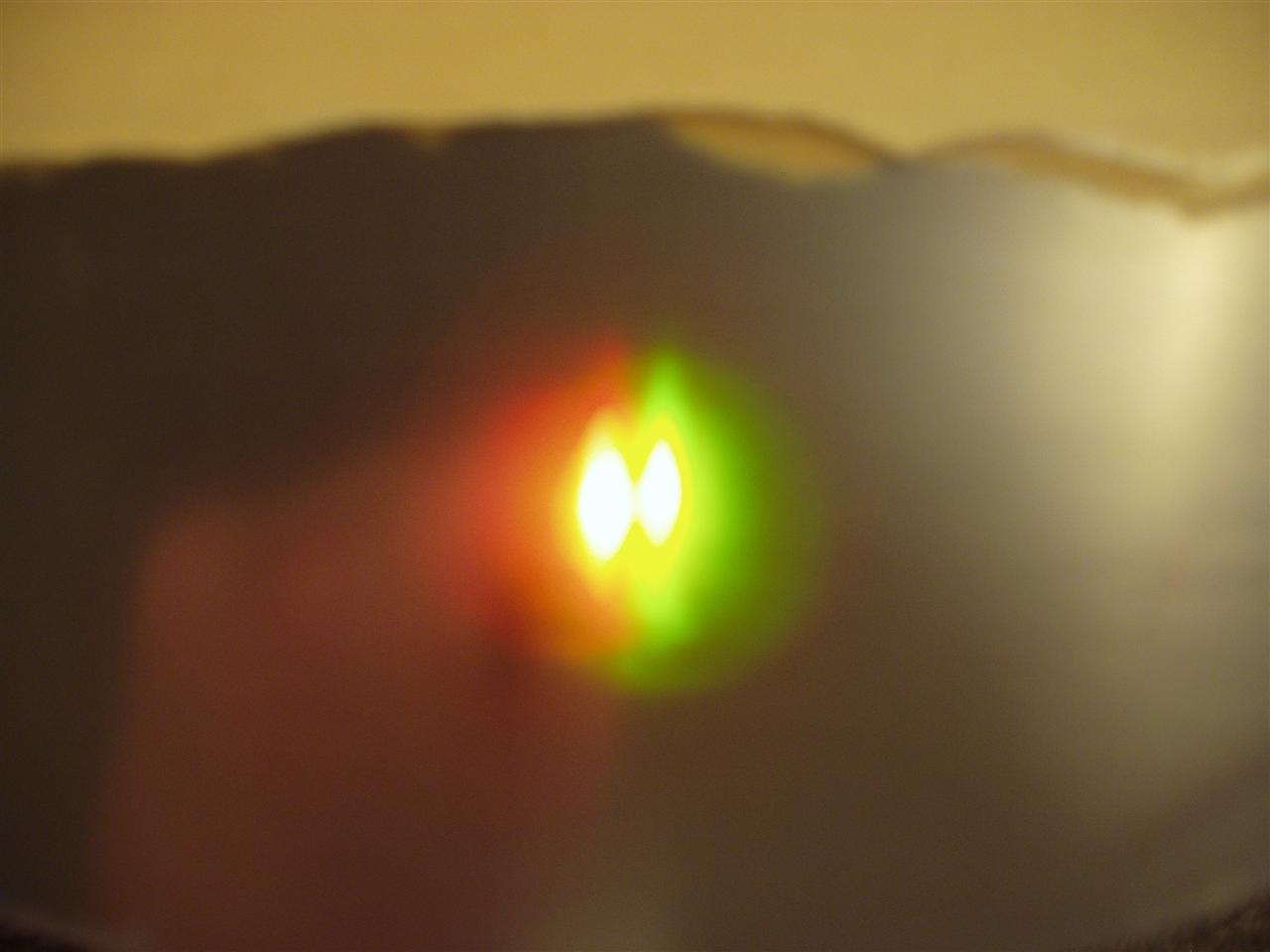
These two pictures demonstrate the before-and-after of my wonderful sanding job on the acrylic. If the pictures were better, they would demonstrate how much translucency it lost after sanding it. You can also see a slight hint of yellow in the last picture (which is what I eventually would want out of red and green LED's. The LED's I'm testing with are just pieces of crap that I had lying around.

Labels: Design
posted by Jurek @ 10:10 PM
![]()
![]()
0 Comments:
Post a Comment
Links to this post:
Create a Link
<< Home